arcing在半导体中的意思是

粉丝9151获赞1.8万
相关视频
 15:58查看AI文稿AI文稿
hello, everyone! welcome back to another video this is video number three of our series of videos in the about packaging the first two videos we talked about packaging traditional packaging technology and the supply chain and how it affects packaging so if you haven't watched those, i highly encourage you to watch those before you watch this, but if you just want to learn about the interposer thanks for joining me today, and let's just get it right on it, so what is an interposer you'll see that here we refer to it as a silicon interposer, and that is because they're mainly made of silicon they can also be made of glass or of garnic organic substrate, but we'll be focusing on the silicon interposer today, and that's why we referred to it as silicon interposer so the silicon interposer it's just a silicon layered between the substrate and the dice as you can see in this picture here, it'll be this this green layer over here, and it is located underneath all of the dies in the package however, it's more than just a layer there for mechanical support it also provides the connection between the dice as you can see by this line here it connects the dies among them, but it can also connect the dice to the ios to the inputs and outputs of the of the package, so it can make connections vertically, but also horizontally and thanks to this it basically eliminates the need for a wire bond, it's a much denser much more efficient shorter connections ah overall better than wire bonds and this is a one of the stepping stones for a two point five and three d technology there's really enabled those technologies to occur, so it does that thanks to the through silicon vias and we'll take a little bit more later on about the through silicon vias, but basically you can think of them as just copper pathways that cross this silicon and they just make the internet connections and that's the that's the technology that allowed all of this to happen now the interposer can be active where he can be passive and we'll also talk about that in a second and like we talked in the previous video the foundries are the ones to deal with all the silicon you know they're the ones to make the wafers so it's no surprise that there are also the ones that make the silicon interposer now, t ismc has been the main supplier of interposers, but other foundries like global foundries are also getting into the market so we should see a big market for interposers in the coming future now why do we need a silicon interposer? you know like you you might be thinking okay that's great, but but why do we need it and basically with newer chips like i said two point five d, three d or chips with just much higher density of interior connections conventional substrate just could not support that amount of pins basically the wire bonds could not a deal with that and the the silicon interposer for the first time allowed a much higher density of interconnections and that just follows morse law you know the chip makers want to make chips with more connection in the tighter space and the silicone interposer was the way to enable that now it's been tested for over twenty years so it's not necessarily a new technology at amp。 t and ibm worked on it in the eighties, but back then it didn't really become popular at all and that's because they had some other laminate substrates that were less dense, but they were had much lower costs so at that point they didn't really need that high density and you know the college was just not worth it however with you know some more modern technology and more time and the market demanding these type of chips with much higher density the popularity if the interposer has gone up it's resurfaced and now it seems to be a key technology in packaging of the first devices that used silicon interposes was this silence verdict seven two thousand t and this was an fpga device and you can see here the insights that uses a silicon interposer to connect the dies so what are the advantages we've mentioned some of them, but let's go more in depth first of all we have a high wiring density because you don't need the wires to be hanging around you can have a much more dense we also have a quiffition of thermal expansion matched to the silicon die, the interposter and the dire both made of silicon which means they have the same coefficient of thermal expansion so that makes sure that there shouldn't be any disconnections between there we also have an excellent electrical and thermal performance for a lower power and this comes with increased band with you know less power usage just better performance overall and this is due to shorter interconnections between the chip and the substrate and as you can see in this diagram to the right for traditional packaging types the signal would have to go all the way through the lead and then through the wire bond into the chip for the devices that use the silicon interposer it can go straight up, and then it goes a little bit horizontally depending on what ship it needs to go to, but the distance is overall much smaller and you don't have any wired and he lose wires around um overall much more efficient so it also you know shorter wires also mean less resistance, which are less losses so it's more power efficient um an overall just much better in terms of performance a wheels have a lower cost of the active of devices because it can petition a large die and finally we also have the possibility of integrating passive devices into the substrate ah like we talked in the previous video system on package sometimes as trying to include some of the devices into the package substrate and the interposure can do that, and also we'll see you later on how active interposures can have active components inside, but let's start let's start from the basic, let's start from the simplest one which is the passive interposer so what does a passive interpose do it acts as an enter connection between the dice and also mechanically it holds all the dice together you will see that all the dice will be on top of the interposer uh, it's like another mechanical layer that holds it all together, but it also provides communication like we said among the dies themselves thanks to the top layer which you can see the top layers in one that goes horizontally and will focus on in a little bit, but also vertically thanks to the through silicon vias and it connects those to the inputs and outputs of the of the chip the passive interpoter has no active devices ah just just connections and therefore i cannot perform any functions ah other than nina connecting the chips to one another uh, the good thing about the packs of interposer and the advantage it has over the active interposer is that it has a higher wiring density and this is due to the fact that um you don't have any devices in the in the silicon substrate to uh block the path of the tsv or you don't have to work around anything it's all free real estate for you to have enter connections now how about the active interposer the active interposer also asks us an interconnection among the chips and from the chips to the package inputs and outputs so the same thing it can be very clean, it can be horse onto lee however, the active interposer has fully functional chips embedded in the silicon like you can see in this image to the right you can have things like a test clock sensors here you can have some components at it um however, we do have a lower density of through silicon vias and this is due to a concept they call the keepout soon now the keepout soon is an air of about twenty microns or so around the through silicon vias where you cannot place any active component because the stress generated by the different thermal expansion coefficient of the copper and the silicon made damaged chips if they are too close to the through silicon vias so we try to stay away from those, but you know as a disadvantage because of that then you have a lot of space that you cannot use and your density will be lower so we've mentioned some of these concerts, but let's look at the structure of the interposer we have three main components that we're going to focus on the first one is the thrucilick and vs or tsv on the thruselaken visa are these yellow bars that connect vertically ah and it just cra goes across the silicon interposer we also have the rdl or the redistribution layer which is the very top layer of the interposer and it's the one that makes the connections vertically and i mean horizontally and they will not only connect the chips to another, but also to the tsvs as needed and finally we have the ubm or under bum metallic station, which will connect solder bumps to the tsvs both from the packets substrate and also from the from the chips so let's look at them a little bit more in depth first of all the tsv through silicon vias it's just a vertical pathway through the silicon interposer you can see here there's not you know that much to it it has a very high aspect ratio they can be under twenty micrometers wide and they can be up to two hundred micrometers stall so it's about ten times as tall as it is wide maybe even a little bit more and a key thing about the the silicon interposters that it needs to have a an angle of ninety degrees or less cause uh we'll see later that the copper is failed so you know in order to not have any bubbles or anything inside the angle will have to be a little bit um slanted so, that there's no no parts that are wearing failed so usually they'll be a little bit thinner at the bottom that they are at the top now how how did they make the tsvs they go through a couple legged simple process where they start by etching the silicon enterposer they make a hole and then they let the silicon oxidate to create an isolator layer and this isolar layer will prevent the current going through the tsv to leak onto the silicon we also have some depositioning where they put some material to prevent diffusion between the copper and the oxide to basically prevent the isolation layer from mixing up and to keep it to keep it you know like new and then we have the filling off the copper where they pour the copper onto the tsv and finally we have some polishing some cmp chemical metal polishing where they get rid of the excess copper and they also reveal the other side of the tsv um by polishing the other side of the back side of the interposer and obviously like i said there is a key pot zone for the active interposer so when you're making your design you have to be very aware of that when you're doing your tsvs let's also take a look at the redistribution layer i can mention the registration layer is all about horizontal connections it's the very top layer of the very top layers of the interposer and like you can see here they just make horizontal connections between the dice, but also they make horizontal connections between the you know between the pins and the tsvs imagine there's a signal that's coming up through this tsv, but it needs to go to this pin over here so the redistribution layers the one the re routes and that's the key concept they reroute the signals to where they need to be and the way they make this is they get a silicon oxide layer that they etch just like they do with the with the tsvs they etch it horizontally and then they let another silicon oxide layer on top of it and then they do as many layers as they need to create the necessary interior connections finally, let's take a quick look at the underbum metallic station so ubm is just a thin pad that connects the solder bump to the copper in the audio or in the packet substrate and you know the audio is just the this small entry connection and the solder bump is a lot bigger in comparison, so the ubm serves as an entry connection between those two and it also prevents diffusion between the solder bump and the and the copper as well as provide mechanical support making a connection and usually these these ubms are made of nickel so now we know a lot about the interposer, but let's take a little bit more of a look into the supply chain so like we mentioned earlier they're mainly made in the foundries ones that make the vias and they make the front side but then there's two possible ways they can be finished they can either continue at the foundry or the idea and they can do a way for support thinning backside bump debonding and shipping or they can send them to the osets and the osets can do those final steps um for them and we can see here in this graph to the left a little bit which companies do each of the processes as some of the bigger companies are teasm sear global foundries which do the tsv ardale and the bumping we also have other technologies like i'm core technologies which doesn't do the tsv but it does rdl bumping packaging and testing and some of the idems like samsung texas instruments sony to shibaibm they can do all of it um so that's a little bit, a little look into the supply chain for the tsvs so quick summary what he will learn we learned that the interposer is a layer that connects the dies it's located between the dies and the package substrate and he connect the dies to each other and to the inputs and outputs like we can see here it gets rate of all the wire bonds it can manage to get things a lot closer together thanks to the reduced revision layer and the high wiring density some of the biggest advantages are again high wiring density we have a thermal coefficient thermal expansion coefficient matched between the silicon die and the silicon interposer we have excellent electrical and thermal performance we have lower cost of active devices and lower power requirements and then we can positively integrate passive devices into the substrate as for the different structure and the different type of interposer we can have the passive interposer and the active interposer the passive interposter has the tsv that goes up vertically the redistribution layer which goes horse ontole at the top of the interposer we have the ubms under mittelization under bummed mittelization that will connect the registration layer to the bumps and then we can have the chips on top of the interposer for the act of interposer all of that still works, but we also have some active components embedded into the interposer which will eventually due to the keepout zone make the tea is redensity lower so that's that's it for today i hope you guys enjoy the video be on the lookout for the following video that we'll be making and have a great day bye bye。
560.7 03:04查看AI文稿AI文稿
为什么静电会产生微发性?在 f 场的各核心工艺模块中,静电几乎无法完全避免,无论是薄膜层激光刻蚀还是离子注入, 都会伴随静电的产生,静电也因此成为贯穿整个制造过程的隐形杀手。但不同制成中静电的成因差异显著,本期星星就带大家拆解习大妈做的静电究竟从何而来。 首先,什么是金源场静电?在 f 场中,静电式制造过程中,因摩擦感应、等离子体工艺等在金源设备、材料及人体表面形成的电核积累与瞬时放电现象,直接威胁芯片良率与可信。接下来我们聚焦五大静电重灾区,分析各个毛作制成中产生静电的主要原因。一、 离子注入区离子注入的静电主要来自三大关键原因,一是高能正离子在传输中聚集形成空间电核效应,轰击金源时会让表面快速积累大量电子。二是离子轰击引发二次电子发射, 电子被撞出后,金元表面正电赫不断累积,进一步加具静电风险。三是用于固定金元的异差所产生的强电场也会带来严重的静电风险。二、刻蚀区这里主要指干法刻蚀过程。静电产生的途径主要有三种, 一方面是等离子体中的电子与离子分布不均,导致金元表面出现电赫积聚,其所谓的等离子体诱导损伤。另一方面是异物差的高压电场 形成静电吸附,可能引发微放电。再者就是传送机械动作产生的摩擦静电也不容忽视。三、薄膜层积 在拍过的等工艺中,其核心的等离子体环境会直接导致晶源表面电和堆积,带来静电风险,这跟刻石有异曲同工之妙。四、光刻光刻环节的静电主要来自两大方面,一是晶源高速旋转及机械运动产生的摩擦起电, 二是惊人于一叉,尤其是 uv 光刻中用到的一百六十 kv 高压甲弹,这吸附与释放极易产生残余电核,引发静电放电。此外,显影、冲洗、甩干等化学液体流动叠 加黄光区高绝缘、低湿度的环境会进一步家具电核累积,增加静电风险。五、司法制程司法制程产生的静电主要有液体流动、旋转、甩干及机械接触分离导致电核分离, 再加上药液反应汉前道工艺产生的电赫共同形成,其中距离止水旋转充,其产生的流动电流电压可达数百至数千伏。而当静电积累至一定程度,就会发生一 s、 d 静电放电。当不同静电电位的物体靠近或接触时, 电赫会在那秒级瞬间转移,电压可达数千伏至上万伏。其中 o、 k、 n 电弧放电是 e、 s、 d 中最剧烈的表现形式, 多见于颗石薄膜层基等等离子体工艺中会直接灼伤惊人,损坏基件风险极高。最后再针对离子注入颗石薄膜层基。光刻和司法制成这五个静电重灾区改善方案,核心在于如何中含静电或把静电导走,主要从工艺参数优化、设备硬件升级、 器件结构调整以及静电消除系防静电涂层与材质等维度展开。静电是大幅场不可忽视的隐形风险。不同工艺模块的产生机理各有不同,却都直接影响芯片良率与可能性。 只有精准把控源头,做好全流程管控,才能有效降低 esd 危害,保障制造稳定与品质安全。本期星星的分享就到这里,欢迎大家在评论区分享交流工作中遇到的相关问题,与进店处理经验,一起探讨更多半导体实战经验与行业干货。点赞关注我们,获得更多资讯哦!
1290Women in tech 02:30
02:30 01:47查看AI文稿AI文稿
家人们,三安光电要爆发了!先看行业地位,它是国内化合物半导体绝对龙头,在 mini led 碳化硅领域试占率超百分之六十,苹果、华为的核心供应商,行业话语权杠杠的。 再看技术壁垒,手握一千两百加项专利,在第三代半导体领域布局超十年生产线,自动化率百分之九十,别人想追至少得三年, 按订单暴增,二零二五年 mini led 订单同比增长百分之八十五,碳化规模快拿下国内新能源车企三十亿大单,下游需求根本拦不住。 二看财务硬实力,去年营收增长百分之四十二,净利润同比飙升百分之五十五,更关键的是,毛利率提升至百分之三十八,比行业平均高十二个点,赚钱效率开挂。 三看产能扩张,厦门、长沙新基地陆续投产,预计二零二六年产能再翻一番。量价齐升的逻辑稳稳的,现在 pe 才二十五倍,对比半导体行业平均四十倍的估值明显被低估。 国家新基建能源政策持续加码,化合物半导体是卡脖子突破关键。三、作为龙头,享受政策加行业双重红利,北向资金最近连续八周加仓,聪明,钱已经动手了,你还在等什么?这可是半导体赛道的潜力黑马, 你觉得三光电今年能涨多少?点点关注评论区扣跟或等,咱们一起聊聊他的后市机会。最后提醒大家,股市有风险,投资需谨慎,咱们只聊逻辑,不见股哦!
 00:55查看AI文稿AI文稿
stm 三二 f 幺零三 c 八 t 六你是不是也好奇为什么他要叫这个名字?每个字母和数字都有什么含义?今天一次性给你讲明白。 开头的 st 代表的是一法半导体,就是生产芯片公司的名字。国产芯片像 gd 开头就是造孽的芯片, hc 开头就是华大的芯片。后续的 m 指的是微控制器单片机, 三十二就是三十二位的处理器。 f 指的是产品的系列,当然也有 h 系列, l 系列, w 系列等等。幺零三指的是具体的子系列,用的是 ko 的 m 三的内核。最后的 c 八 t 六 c 代表的是它有四十八个引角。八 它表示的是 flash, 容量是六十四 kb t 代表的是四边形分装。六就是工作温度的范围。理解芯片型号是第一步,真正想玩透它,还得系统学会如何驱动它的各个外设。我整理好了一份 stm 三二常见的外设思维导图,总结了常用的知识点,需要的同学留言六六六。
42嵌入式六哥 05:42查看AI文稿AI文稿
昨天大魔出了一篇关于大中华区半导体的报告,这篇报告信象很大,我先给你们说一下它的核心结论啊,非常直接,就是现在 tpu、 gpu 还有存储继续走强,但是另外一边呢,智能手机和 pc 相关的半导体,反而面临更大的压力。 这话听起来很简单啊,但其实背后想说的是,现在的半导体行业,它不是全面复苏,而是一个非常典型的 ai 强、传统弱的结构行情。 什么意思呢?就是现在跟 ai 相关的那部分啊,景区路都在往上走,但是传统消费电子,比如说手机、 pc 这块,其实恢复的并不扎实。大摩在这篇报告里面写的很明白啊,他更看好三个方向,第一个是存储,第二是 ai 和数据中心半导体, 第三就是 c p o 的 相关链条。那为什么会这样呢?因为现在 ai 已经不只是带来新增需求了,开始抢资源了。 你可以理解为 ai 正在红吸整个半导体产业链的资源,它不只是需求更强,现在连供给、产能分装、资本开支,大家也都在优先满足 ai, 而不是非 ai。 这个事很关键啊,因为以前很多人觉得这个 ai 景气上来之后,整个半导体行业会一起受益。但是现在越来越清楚了,现实并不是这样, 真实的情况反而是 ai 越强,非 ai 的 那部分可能越沉压。大模的报告里面给了很有代表性的两个数据啊,第一个就是如果我们剔除英伟达的 ai gpu 收入,二零二四年非 ai 的 半导体增长只有百分之十。第二就是逻辑,金源代工厂的加动率到二零二六年上半年也大概只有百分之七十到八十。 你把这两个数据摆在一起,你就能看的很明白了,现在半导体的景气,它不是传统需求自己回来了,而是 ai 单独把整个行业景气度往上拉了一大截。所以啊,从投资角度来看呢,最重要的已经不是笼统的说一句我看不看我半导体这么简单了,而是你要先分清楚,你看好的它到底是不是跟 ai 沾边的那一边。 所以啊,这份报告里面还有一个特别的核心,就说的是台积电。大摩有一句判断,我觉得非常值得记住啊,他说 ai 不 管最后赢的是 gpu 还是 sx, 台积电都会受益。这个逻辑其实很好理解,我也在视频里讲过很多次了,因为不管是英伟达这种通用 gpu, 还是谷歌、亚马逊、微软这些厂商,它自己做的定制芯片,最后都绕不开这个先进制程,先进封装。而台积电呢,正好卡在这个最核心的位置。 这份报告还预计啊,到二零二六年呢,台积电的 ai 半导体收入占比可能超过百分之三十。同时呢, kolos 产能到二零二六年可能扩展到十二点五片每个月。 所以你如果问我这轮 ai 的 半导体锦旗里面,谁最像卖铲子的核心资源,台积电还是最绕不过去的那个。然后这篇报告还有一个点,我觉得市场可能低估了,就现在这个存储,它不是陪跑,反而是 ai 行情里面可能最硬的方向之一。大摩对存储明显是偏乐观的,它提到啊, ai 存储会带来 nine 偏紧, norflash 到二零二六年也可能会供不应求, ddr 四短缺可能持续到二零二六年的下半年。这背后说明一件更重要的事情啊,就很多人现在一说 ai 存储,第一反应就是 hbm, 但是大魔这篇报告其实是在提醒你, ai 带来的影响,它已经不只是 hbm 了,而是现在往更广阔的存储品类外溢,比如推理场景起来之后,长上下文, k v 缓存、数据搬运编预测存储,这都会把更广泛的 n 的 需求往上拉。报告甚至测算啊,二零二六号,二零二七年, ai 推理相关平台会额外带来百分之一和百分之十三的 n 的 消耗, 这就意味着什么呢?因为 ai 现在不只是历好最尖端端的假韩国公司,它已经开始把需求往更底层、更大范围的存储层传导了。再往下看云厂商资本开支这块,这篇报告给的判断也很明确,现在钱还在继续花, 而且呢,花的还并不少。这报告里面提到了亚马逊、谷歌、微软、 mate 这四大云商,二零二五年四季度的资本开支同比增长了百分之六十四。同时预计呢,二零二六年全球十大云厂商的资本开支接近六千八百五十亿美元。 这个我已经在无数的视频里面讲过这个问题了,这其实是在回答市场一个非常现实的问题,就 ai 这波,它到底会不会开始熄火?云厂商会不会缩减 capx? 那 至少以目前的判断来看,答案是不是? 而且呢,还有另外一个趋势啊,就是后面可能越来越重要。未来这些 ai 半导体的增量,它不只是训练级 pu 了,更来自推理和 sx。 这个我也是讲了很多遍了,你们长期跟进我的视频的朋友应该都能理解这件事情。 摩根施丹利给了一个长期的预测,他们预测边缘 ai 半导体二零二三到二零三零年的年复合增长是百分之二十二,推理型的 ai 半导体呢,复合增速是百分之六十八, 定制 ai 芯片的复合增速是百分之六十五。这个话很重要,因为它其实是在告诉你,下一个阶段不要只盯着英伟达一家公司,而是你要顺着这个产业链继续外扩,看 asset, 看 hbn, 看 cpo、 看测试和后段分装。 也就是说什么呢,市场主线啊,现在正在从单一的 gpu 龙头慢慢开始走向整个 ai 的 算力基础设施。最后再说一下我们大陆这部分啊,大摩给的判断是, deepsea 带来的低成本推理,现在正在刺激我们 ai 的 推理需求,也会带动后续的资本开支。并且预计国内头部的六家公司二零二六年的资本开支同比增长百分之十一到四千四百五十,那到了二七年的有望提升到百分之五十。 也就是说,本土 gpu 的 收入到了二零二七年可能达到一千三百六十亿人民币。但是这里呢,留了个变量啊,就如果因为达到 h 二百还能继续出货,那本土 gpu 链条的弹性可能会被减弱。 所以啊,咱们国内这块投资上更像是看两条线同时再走,第一条是推理需求起来,带动 kpx 继续上行,另外一条是国产的 gpu 替代,带来产业链的弹性。 我自己把这篇报告最后归类成一句话啊,就是半导体现在不是一个全面优势,它是一个 ai 独强,现在谁离 ai 的 算力先进,制程先进,分装 hbm 测试更近,谁就更强, 但谁更依赖手机、 pc 这些传统需求,谁就容易继续沉压。所以接下来真正重要的是不是问半导体还能不能买,而是问你买的到底是 ai 链还是传统链。这两个世界现在越来越不像一回事了。
738蛇口费雪和不二家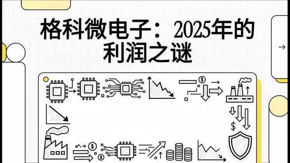 05:32查看AI文稿AI文稿
今天我们来聊聊一家半导体公司,格科威电子,他们二零二五年交出的这份成绩单啊,有点意思,甚至可以说是挺矛盾的,这背后到底是怎么一回事呢? 你看,这就是问题的核心了,一边是营业收入蹭蹭往上涨了百分之二十多,另一边呢,净利润呢?哐当一下掉了七十,百分之还多,这就奇怪了对吧?卖的东西多了,赚的钱反而少了。 咱们今天就来把这个事掰开揉碎了看看。好,那咱们先看好消息,这个营收增长到底是怎么来的?是什么在背后推着他跑呢? 我们来看看这份年报的招标,你看,这个营收增长是实打实的,不是虚的。而且最关键的是什么呢?这增长几乎全都是靠他们的主营业务,也就是卖图像三 sir 赚来的,可不是靠什么一次性的收入撑起来的场面, 那成功的秘诀到底在哪?其实说白了,就是他们成功杀进了高像素 cms 图像深 sir 这个市场 啊。这个东西听起来可能有点专业,但他就是咱们智能手机摄像头里那个最核心的零件,负责把光变成图像,像素越高,你拍出来的照片就越清楚,就这么简单, 这个数字就更能说明问题了,超过一亿颗。你想想,光是一年,他们就卖出了超过一亿颗,这种高像素的深色的,说明他们在市场上的渗透力真的很强。 好,那问题又回来了,既然卖的这么火,钱呢?利润到底跑哪去了呢? 嗯,根据公司自己的说法啊,这利润下滑背后主要是三个元凶,一个是定价策略,一个是汇率,还有一个是非经常性献物的影响,咱们一个一个来看。 首先啊,就是定价,你想啊,格克威在高像素这个高端市场里算是个新玩家,要想挤进去,最直接的办法是什么?就是价格战吗?用一个比较有竞争力的价格来抢地盘,抢市场份额, 但这么做的代价就是每一件产品赚的钱,也就是毛利率,自然就下来了。第二个原因,汇率。 这个也挺要命的,你看啊,他们很多生意都是用美元结算的,但是在二零二五年呢,美元对人民币一直在贬值,这么一来一回,账面上的钱就白白蒸发了不少,这就叫汇兑损失。 第三个原因呢,听起来有点绕,叫一次性项目,说白了就是去年的利润里头包含了一笔比较高的政府补贴, 这笔钱一下就把去年的利润基数抬高了,所以今年再一笔,就算今年的经营情况没那么差,这个降幅看起来也会特别夸张。就是这么个道理, 讲到这,我们听到的都是公司自己的解释,那那些天天研究这些公司的专业分析师们,他们又是怎么看的呢? 他们的视角可能会给我们一个更宏观的途径。有意思的地方来了,你看,虽然利润暴跌,但是像中邮证券这样的机构出的报告居然还是维持买如评级, 这又说明什么?说明在他们眼里,这事啊,没那么简单,不能只看一年的利润数字,你看分析师们好像根本不在乎短期的这点利润波动,他们更关心的是一个大趋势,就像这本报告里写的这几个字,五是 m 持续上量, 什么意思呢?就是他们家最高端的五千万像素仙子出货量还在蹭蹭浪的往上涨,这才是他们眼里的未来。 而且报告还特别提到了格科威一个很关键的战略转型,叫 fablite 模式。这个 fab 呢就是指芯片制造厂,所谓 fablite 就是 轻制造的意思, 它们既有自己的工厂搞一部分生产,同时呢也把另外一部分生产外包出去,这样一来就特别灵活,可以说是进可攻退可守。 那这种模式具体好在哪呢?你看,首先有了自己的工厂,从设计到制造就能更好的整合自己说了算。 其次能给那些顶级的大客户做一些定制化的产品,满足他们的特殊需求。最后因为一部分生产是自己的,就不用花那么多钱出去招人代工了,手里的钱就更宽裕。你看这策略是不是把控制力和灵活性都给拿捏住了?好了,说了这么多,咱们来总结一下, 从这些信息里,我们到底能看到一个什么样的关键结论呢?其实答案已经很清楚了,格科威现在正在做的事情就是一场豪赌,他们赌的是未来,赌的是市场份额要远比短期的利润更重要, 他们这是在用今天的钱去买明天的市场地位。所以你看,这个战略就完美解释了我们一开始看到的那个收入和利润的矛盾。 但这也留下了一个更重要的问题,不光是给格格威的,也是给所有在激烈竞争中的科技公司的。 用眼前的利润去换去未来的市场,这到底是不是一部好棋?这会不会是一个制胜的策略呢?我想只有时间能给我们最终的答案了。
21🐶来💰 00:38查看AI文稿AI文稿
芯片上这么多引脚,到底是什么意思呢?今天呢,一分钟带你搞懂芯片引脚!字母分六大类,先讲最常见的电源接力类, vcc 呢,是双极性电路电源正极, ve 呢,是双极型电路电源负极, vss 是 末磁电路电源负极。 vpp 呢,是编程烧录电源引脚。 a、 g、 n、 d 呢,是模拟电路地线, d, g, n, d 呢,是数字电路地线。其他还有输入、输出、控制、信号等五类。后面呢,慢慢聊,搞懂这些选行,看图纸都能少走弯路!
20炬微半导体 04:37查看AI文稿AI文稿
大家好,我是 fly mood。 又到了每周半导体新闻时间,这周有三个大新闻,每一个都可能改变行业格局。简单说就是台机电和 intel 在 二纳米技术路线选择上神仙打架, apple 和 nvidia 用脚投票,还有一场你绝对想不到的合作, 我跟你讲,这里面信息量巨大。第一个新闻,台积电 ceo 最近说了句很硬气的话,他说我们二纳米不用背面供电,技术也比 intel 十八 a 先进。这话什么意思? 简单说就是 intel 这两年憋了个大招,叫背面供电 power wire, 媒体都说 intel 要靠这个反超台机电,结果台机电 ceo 直接回应,不用这招,我也比你强。背后是数据的支撑。台机电二纳米晶体管密度三百四十 m, intel 十八 a 大 概三幺三 m, 台积电领先百分之八点六,这意味着同样大小的芯片,台积电能多塞百分之八点六的晶体管。对于 apple 这样的客户,芯片面积就是钱, 但 intel 也不是没机会, intel 的 背面供电能把电压降降低百分之三十,数据上同样功耗下, intel 性能提升百分之二十五, 台积电只有百分之十五。现在的问题是客户怎么选? apple 已经确认,二零二六年的 a 二十 pro 用台积电二纳米, nvidia 的 blackwell 后续版本也用台积电,只有 microsoft 和 qq 用了。 intel 十八 a, 说白了,下游更看重量产时间和量率,而不是单一技术。亮点。 第二个新闻, intel 十八 a 确实量产了 panzer lake 处理器,二零二六年 q 一 上市,成为业界首个背面供电商用芯片。但关键数据来了, 良率初期传闻只有百分之十,现在 intel 说提升到百分之八十了,但客户要看到实际出货。如果良率真能稳定在百分之八十,加 intel 可以 在二零二八年抢到百分之二十五到三十的市场份额,但如果良率上不去,就尴尬了。 第三个新闻,你可能想不到, samsung 和 intel 这两个老对手居然合作了。为什么?为了对抗台积电, samsung 的 二纳米技术叫 s f 二,良率一直上不去,只有百分之五十左右。 intel 有 备免供电技术,但产能有限。 两家一合计, samsung 负责前端制造, intel 负责后端封装,各取所长。这个合作如果成功,二零二七年可能形成台积电、 intel、 三星三足鼎立的格局,但关键是良率,良率!良率!重要的是说三遍。第四个新闻来自 ai 芯片领域, amd 和 mate 宣布扩大合作,要部署六级码的 amd gpu 什么概念?相当于二十万张 h 一 百,关键是时间点,二零二六到二零二七年。这说明什么? mate 对 amd 的 mi 四百系列 gpu 有 信心,愿意大规模部署。另一边, nvidia 的 新芯片传闻二零二六年底发布,性能提升百分之四十,但价格也涨百分之三十。 现在的问题是, amd 能否趁 nvidia 涨价的机会抢下更多市场份额。我的判断是短期不能,但长期有机会,因为生态, nvidia 的 qda 生态太强, amd 要追赶需要时间。第五个新闻,存储芯片还在涨价, dream 价格连续三个月上涨, nand 也涨了百分之十五,原因是 ai 需求爆发, hbm 三亿供不应求,价格涨了百分之五十,受益方三星、海力士、美光。但这里有个风险, 当 ai 训练需求饱和后,价格可能暴跌。关键时间点,二零二七年下半年。最后说说咱们能投什么? a 股的话,关注两个方向,第一个是通富微店,代码零零二幺五六,它是 amd 的 核心风侧商,如果 intel 十八 a 成功了, 先进封装需求会提升,它受益。第二个是中微公司,代码六八八零幺二,它是刻蚀设备龙头, 不管台积电还是 intel 量产 g a a 纳米片制成的课时步骤都增加百分之三十以上,它都受益。但话说回来,半导体周期波动大。 beyond 总结一下这周的新闻,核心就两个词, 良率合作。台积电靠密度和良率领先, intel 靠新技术追赶,三星靠合作求生。二零二六到二零二七年,二纳米大战正式开打,谁能赢? 看量律数据。关注我,我是 fly mood, 一个在半导体行业摸爬滚打的芯片工程师,每周为你解读最新行业动态。
 02:21查看AI文稿AI文稿
比如说金属的一些电的特性我们是很清楚的,半导体的电的特性其实我们也有所研究,但石敏教授更多是在研究这两者的界面上。当金属和半导体进行一个导通的时候,在界面上的一些东西就是跨越两个不同的材料之间,他的一些特性,应该是这个意思,对吧? 界面是一部分,他本身接触的话就成了一个整体了吗?我们任何的一个元器件也好,就是在集成电路里边的摩斯管也好,其他的二极管呀等等啊,包括这个三极管啊, 还有我们的功率电子学呀啊,那么里边的这些器件的话,他都需要和外部电路去连接,那么通常我们都是用金属和半导体做一个 接触,那么这种 om 接触的话就是连接的一个方式。我举这个例子就是说我们考虑啊,门内个门外哈,一个在门里面,一个在门外面,假如说我们希望这个水啊也从门里面往门外流和门外往门里流的时候,你可以流动吗? 它流动的它有几种情况,一种呢是门里面和门外面,它的水平面,它的面是一样的啊,就是高度是一样的, 那这个水不管从门里面流向门外面还是门外面的流向门里面都是可以流的,对吧?只要你有水,他就开始往里面方向走, 这种的就是相当于欧盟接触的感觉,这个水可以流来流去,里到外流,外到里流都可以,这是欧盟接触。 第二种呢,假如说我们里面的这个高度跟门外面的高度不一样,那不一样的情况下呢?这种说我们这时候还有一个因为各种各样的原因啊。啊?还有个门槛,那这种情况下呢?如果说从高处往低处的时候呢? 看着门槛多高啊?门槛低一点他可能就或者说完全没有门槛,他就可以从高处往低处流,但是如果说是有门槛,从低处往高处他就就流不了了,但这个门槛还可以调节哈,这就是销售销的第四类的感觉哈。但是这里面我觉得是一名教授做了一个特别重要的工作的,就是很系统的分析啊,怎么样去? 呃,就系统的分析研究这个门槛的高度是什么原因决定的,材料的特性,还有界面态的原因,界面里面的各种各样的状态等等啊,有很有很多因素掺杂等等。那只通过什么方法 啊?可以把门槛给他降低一点,高度差降低一点,让我的水可以里外流的更顺畅一点。
11未来论坛 01:50查看AI文稿AI文稿
打开这个软件,我们会看到三个东西,一个是位置,一个是力,一个是速度,这就是对应的刚刚说的三黄位置黄,位置黄的意思是什么呢?它这里会有个百分之百,百分之百的形成,这里的话位置黄是可调的,比如说调到百分之百分之十,你可以看一下,它就会关到百分之十这里,然后我要调到百分之二十五, 他就会打开到二十五,这就叫位置打开了吗?打开了再调一下五十,然后就是吧,嗯,对器爪来说的话,他的位置的话,他一般基本都是零到一百,对,调不了,对,这就是一个位置哈。然后力,力的话,力的话也俗称电流环,为什么要说电流环呢?因为电流环的话,他是这个力是通过电流去控制的,他不是通过力的传感器去控制的,所以说他叫 电流滑。嗯,然后他这里的力的话也是可调的,这里是百分之百的力去加,我要调百分之五十的力去加,嗯,他就这里是可调,这里面就是力可调,这里调好了,比如说你下次要加的时候,他就是用百分之五十的力去加,嗯,他是百分之百的力去加,然后这里还有一个就是速度滑,嗯,速度滑的话就是他的一个 一个夹死的一个速度比刚刚是百分之百,百分之百的速度去加,如果说我要调小一点,不要加那么快,这里就可以调,嗯,这就是所谓的 锐志环、电流环和速度环。那你旋转的话,他会有两个,两个参数是比较重要的,一个就是力矩,就是他的一个多大扭力,嗯,然后他这里会有个速度吗?就是一个旋转速度,旋转速度,这就是旋转速度。嗯,然后他这里会有个旋转角度,看到没有?他这里会有个旋转角度。你说我先给他旋转个一千八百, 他就会转个一点八百度。就是比如说有些应用场景是怎么样呢?我要转这个东西,我要,我要抓这个东西,我转多少圈?比如我要转九十多二百七十度,还是说是五百四十度?他这里是可以这样子运用的,就是他的一个角度,他的旋转角度这方面是可以调的。是,然后他这个力也是可以调的。好, 这个速度的话也是也是以百分之百的速度去调,还是说是多少速度去调?这也是可以调的。好,那我现在要求旋转七百二十度,嗯,力的话是百分之五十,速度百分之八十。对啊,就可以直接直接可以调,调一下,看一下。那你先回零嘛?一般然后调七百二,然后就可以,然后就可以就可以回形了。你没看他的速度明显慢了吗?是,这就是一个大概的一个应用。嗯。
 02:08查看AI文稿AI文稿
哈喽,大家好呀,这几天关注中韩半导体 etf 的 朋友或许已经看到了他的溢价风险提示公告,截止三月四号收盘呢,产品在二级市场的溢价率已经达到了百分之二十五点五的历史最高水平。 那么这个溢价是什么意思呢?因为 etf 存在两个市场,一级市场身熟的价格反映底层资产的价值,也就是 i o p v。 而二级市场交易价格通常由买卖双方竞价决定,当过多资金通过二级市场买入时,交易价格会被推高,形成对 l p v 的 溢价。今年以来呢,韩国股市在全球资产中表现较为突出,这与全球 ai 算力建设加速, 对高宽带存储器的需求持续增长有关。中韩半导体 e t f 是 目前 a 股唯一可直接投资韩国市场的 e t f 产品,这种稀缺性呢,使得活跃资金对于中韩半导体的投资情绪高涨,所以推高了交易价格。 但是近期呢,韩国市场出现调整,其净值随之下行,二者共同作用导致溢价率进一步走高。需要说明的是呢,作为跨境 etf, 它的运作受 qd、 额度等因素约束,常规的 e 二级市场套利机制难以充分发挥作用, 这也是溢价得以持续的技术性原因。那么,在 etf 大 幅溢价时买入有什么风险呢?这时付出的成本就可能会高于 etf 的 底层资产价值, 很有可能是在为高昂的市场情绪买单。高溢价买入的投资者,即使基金净值没有波动,当溢价回落时,也可能面临本金亏损。同时呢,还需关注底层资产波动、流动性、汇率等多重风险。 今年以来,我们已累计发布了五十六次溢价风险提示公告,也采取了临时停牌、收紧链接基金的申购等多项措施。这里也要再次提醒各位投资者,务必关注产品溢价水平和官方的公告,结合自身的风险承受能力理性投资。
 06:43查看AI文稿AI文稿
大家好,今天咱们来聊一个最近特别火的话题,一个听起来有点科幻,但又实实在在撬动了市场几百亿资金的神秘策略 fellow。 不知道你有没有发现,最近市场画风突变,一边是中东占云密布,国际油价蹭蹭往上涨。另一边 a 股里那些传统的大家伙, 石油、煤炭、有色金属、电网设备突然成了香饽饽,资金像潮水一样往里涌。而之前风光无限的 ai 半导体,反倒有点眼旗吸股的意思。这背后其实是一场席卷全球资本市场的策略大迁徙。它的名字就叫 hallo。 你 可能要问了,这 hallo 到底是个啥?是天使头上的光环吗?跟投资有啥关系?别急,我告诉你,它可比天使的光环硬核多了。 简单说, hello 就是 重资产低淘汰的英文缩写,它瞄准的是那些 ai 啃不动、搬不走也替代不了的硬核实体资产。想想看, ai 再厉害,它能挖矿吗?能发电吗?能建电网吗?能炼油吗?不能! 这些需要巨大实体投入,技术迭代极慢,但又为整个社会,尤其是为 ai 本身提供物理血液的行业, 就是 hello 策略的核心。那么这个策略有多火呢?我给你几个数字,你感受一下。就在春节假期回来后的短短五个交易日里,超过一百九十亿元的资金疯狂涌入了与 hello 策略相关的 etf, 比如油气 etf、 化工 etf、 有 色金属 etf 和黄金 etf。 光是三月二号这一天,单日涌入的资金就超过了一百二十亿元。这可不是小打小闹,这是真金白银在投票。 更有意思的是,全市场有十五只权益 etf 在 春节后获得了超过十亿元的资金净流入,而流入的方向只有两个, 一个是哈喽策略的相关 etf, 另一个就是以恒生科技为代表的港股科技 etf。 市场资金正在用角投票,进行一场极致的杠铃式配置,一头压住未来科技的弹性,另一头则牢牢抱紧这些实体资产的压仓时。为什么是现在? h a l o 策略的突然爆火,其实是三重焦虑叠加的结果。第一重是 ai 颠覆焦虑。过去几年, ai 的 故事讲得太美,估值也飞得太高。但大家慢慢发现, ai 在 颠覆别人的同时,自己也是个电老虎、资源吞食兽, 他越发展,对电力、对数据中心、基建、对铜铝这些原材料的需求就越大。于是,聪明的资金开始思考,与其去赌哪家 ai 公司能最终胜出,不如去投资 ai 离不开的卖水人。那些为 ai 提供底层支撑的硬资产公司。 高盛和摩根士丹利这些华尔街大行今年初就开始大力推广这个逻辑。第二重是通胀年性焦虑。 全球范围内的再通胀预期一直在,而最近的中东冲突就像往火堆里浇了一桶油,霍尔木兹海峡的航运风险直接推高了油价和全球供应链的紧张情绪。在这种环境下,拥有实物资产、能直接受益于价格上涨的资源类公司,自然就成了资金的避风港。 第三重是地缘不确定性焦虑。黑天鹅事件频发,世界似乎变得越来越不确定。在这种时候,那些业务模式稳定、现金流可预测,并且身处大国核心利益领域的重资产公司就显得格外可靠。所以你看, hollow 策略的火爆根本不是偶然,它是资金在 ai 狂热、高利率和地源动荡的复杂环境下,一种本能的求生选择,去找那些踢得着、看得见,并且 ai 和战争都很难摧毁的东西。摩根士丹利基金的基金经理就明确表示,他们一直以来的策略就是 ai 加 hollow, 摊好 ai 基建以及电力设备、数据中心、半导体设备等方向。这给了我们一个非常重要的行业洞察。未来的投资可能不再是简单的新旧对立,传统产业和新兴产业正在深度融合, 那些为 ai 为新能源提供核心材料和基础设施的老树正在发出新芽,它们的价值正在被市场以成长的逻辑重新评估。聊了这么多,最后咱们落到实际的投资上。如果你对 hello 策略感兴趣,该怎么看?又该怎么参与呢?首先要理解它的本质, h a l o 不是 短期的题材炒作,它是在宏观大背景下的一种资产配置思路,它适合那些追求稳健、希望对冲高波动,并且看好实体经济长期价值的投资者。其次,普通人参与最便捷的方式就是通过相关的行业 etf。 从资金流向看,几个主要方向非常清晰。 第一个是能源与材料,这是哈喽的核心,包括跟踪油气产业、有色金属、化工等指数的 etf, 比如华夏的电网设备 etf、 国泰的油气 etf, 都是近期吸金的大户。第二个是公用事业与基础设施,比如电力、港口、航运等,这些行业具有天然的垄断性和稳定的现金流。 第三个是与 ai 强相关的上游,比如为数据中心提供散热服务的液冷、提供电力的储能和变压器等, 这些是直接受益于 ai 资本开支爆发的卖水人。但是,投资哈喽策略也必须清醒地看到其中的风险。 第一,短期交易过热的风险。像三桶油这样的公司已经连续涨停,并在昨晚集体发布了股价异动公告,提示油价波动风险。任何资产短期涨得太急太快,都积累了回调的压力。第二,对宏观环境的高度依赖。 这个策略成立的前提是通胀预期、地源紧张和 ai 资本开支周期持续。如果其中任何一个因素发生逆转,比如地源局势突然缓和,或者全球陷入通缩,逻辑就会受到挑战。 第三,它并非成长股的替代品。 h a l o 资产的优点是稳健,缺点是想象空间相对有限。它更适合作为你投资组合中的压仓石或稳定器,而不是全部。 所以,我的建议是,对于大多数投资者可以借鉴机构正在实践的杠铃策略。在你的组合里,一部分配置代表未来方向的 ai 科技成长作为进攻端,另一部分配置 hello 相关的硬资产作为防御端, 两者的比例可以根据你的风险承受能力来调整。在市场波动加大、前景不明时,可以适当向 hello 这一端倾斜。当市场风险偏好提升、成长主线清晰时,则可以增加进攻端的藏位。 记住,没有一种策略能永远赚钱。 k l o 策略的兴起是市场在特定时期寻找确定性的结果。它的核心启示在于,在技术飞速迭代、世界充满不确定性的今天,那些构建我们物理世界基石难以被复制和替代的硬核资产,正重新获得资本的青睐。
84妙喵股事局


猜你喜欢
- 1221通讯人小旭
最新视频
- 1.7万主持人阿喆